
New features: “Layer editor” and “Buildup wizard”
Two new functions extend the power of PCB Visualizer: “Buildup wizard” and “Layer editor”. The Buildup wizard allows you to add blind and buried vias into one of our 700 pre-set multilayer builds. Layer editor allows you to map your files to their types or functions in a build. Together they bring new functionality to our smart menu concept. PCB Visualizer gives you a more accurate analysis of your data and a more accurate price. Your job goes into production faster without any delays caused by data issues.
Layer editor.
The new Layer Editor can be accessed in the import section in PCB Visualizer and in the PCB Configurator price calculation menu where is resides within the Buildup wizard under Layer Mapping. It allows you to interactively link data files of layers to their type/function in the buildup.
In PCB Visualizer theLayer Editorperforms a dual function. Every year we receive over 40,000 new designs from around 12,000 designers. Not all of them are able to follow our recommendations on file naming which prevents PCB Visualizer to be fault less on layer assignment. Using the Layer Editorthe designer can assign the layers manually or correct PCB Visualizer’s tentative assignment. Correct Layer mapping results into an accurate analysis of the board data and a correct price.
At the same time, PCB Visualizer is learning new assignment rules. The algorithms that it uses for Layer mapping are based on thousands of examples, collected over several years. Every new manual assignment is stored and analysed by self-learning software within the program so that more data sets can be read correctly in the future.
The Layer Editorcan be used prior to calculating a price when using the option “Analyse your data”. Upload your files and if there are any layer assignment issues, you can usethe Layer editorto resolve them. If there are other data issues flagged up by PCB Visualizer, for example, fine tracks or gaps, use PCB Checker to pinpoint each one. You can then modify the design data if required, or use the measured values shown PCB Configurator. In any case you get a more accurate quotation. If you add blind or buried vias usingBoard buildup, a drop down containing your data files will be available in the “layer mapping” tab, so that you can assign the drill files in your dataset to the newly created blind/buried vias in the buildup.
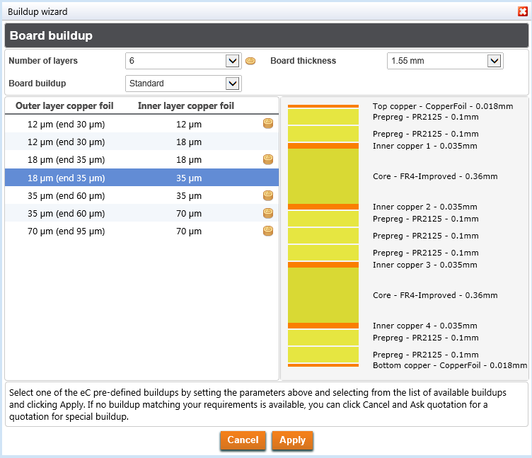
Buildup wizard.
The new Board buildup function works inside the Buildup wizard which can be found in our price calculator and in PCB Configurator. You can choose from over 700 pre-set multilayer builds, accessed by number of layers, board thickness, build and copper weight. If you can use a pre-set build you get your offer faster, the boards are easier to build and so the price is lower.
Board buildup allows you to add blind and buried vias using a simple interactive menu . However, not all combinations of layer builds and blind/ buried vias can actually be made. We know that pressurized designers do not have time to work out in detail what is and what is not possible. Our smart menus allow us to share our fabrication knowledge with you as a board designer in an efficient and effective way. So the Board buildup software includes automatic validation functionality. This immediately flags up invalid combinations with a clear explanations of what is wrong.
Blind vias correct.

Blind vias incorrect
Use Board buildup to find what combinations of builds and blind/buried vias are possible, to verify your designs and to evaluate the costs of the different possible combinations. The result? Your board goes into production quicker, you eliminate design re-spins due to manufacturability issues and you get the most cost-effective combination of price and technology.
More information on Board buildup and Layer editor


